A video installation referring to the parallel between real and digital transport.
Made for GS1, a not-to-profit organization known for their work on the barcode (!), France, 2020-2021.
Relation to GS1
– Traceability
The traceability solutions of GS1 are translated into the work by making use of copper-traces. These copper-traces are usually part of an electronic circuit in a printed circuit board (PCB). The traceability-aspect is quite literally present in the work.
– Transparency
The installation makes use of the transparent properties of the materials. The PCBs are very thin and light is able to shine through them. The LCD-screen uses pixels to block light at certain areas.
– Circular, collaborative economy
The generated traces are used for showing forms of traffic / transportation, which looks similar to traderoutes. It’s mimicking transport from countryside to a city, and visa versa, or in a circular pattern.
– New technology
The theme technology is very visible in the material by using a designated technical material.
The composition and visuals of the artwork are generative, meaning that it’s all algorithmically generated.
About the material: printed circuit boards
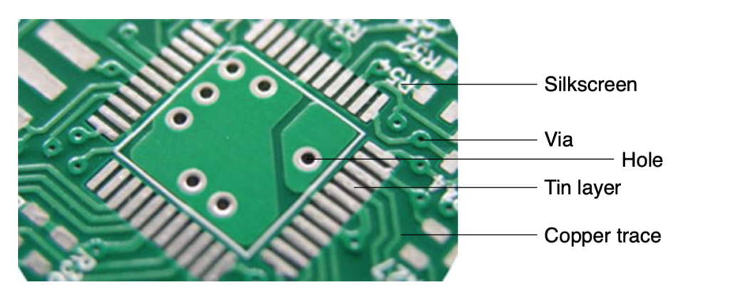
PCBs are made of a glass fiber reinforced epoxy resin with copper traces running through it. These traces are normally used for transmitting electrons which are mainly used as signals for computers. Most common are two-sided PCBs, with traces on the top and the bottom.
The traces are only visible from one side, but by lighting the back of the PCB the traces on the other side will also become visible.
On the top of the PCB there are tin pads and holes, used to place components (resistors, capacitors, transistors, etc) upon or through.
Besides the tin layer there’s a white print (silkscreen), to indicate the position of the components and other information.
All these layers will be used for the canvas of Tracing.
Design process
Intro: setup
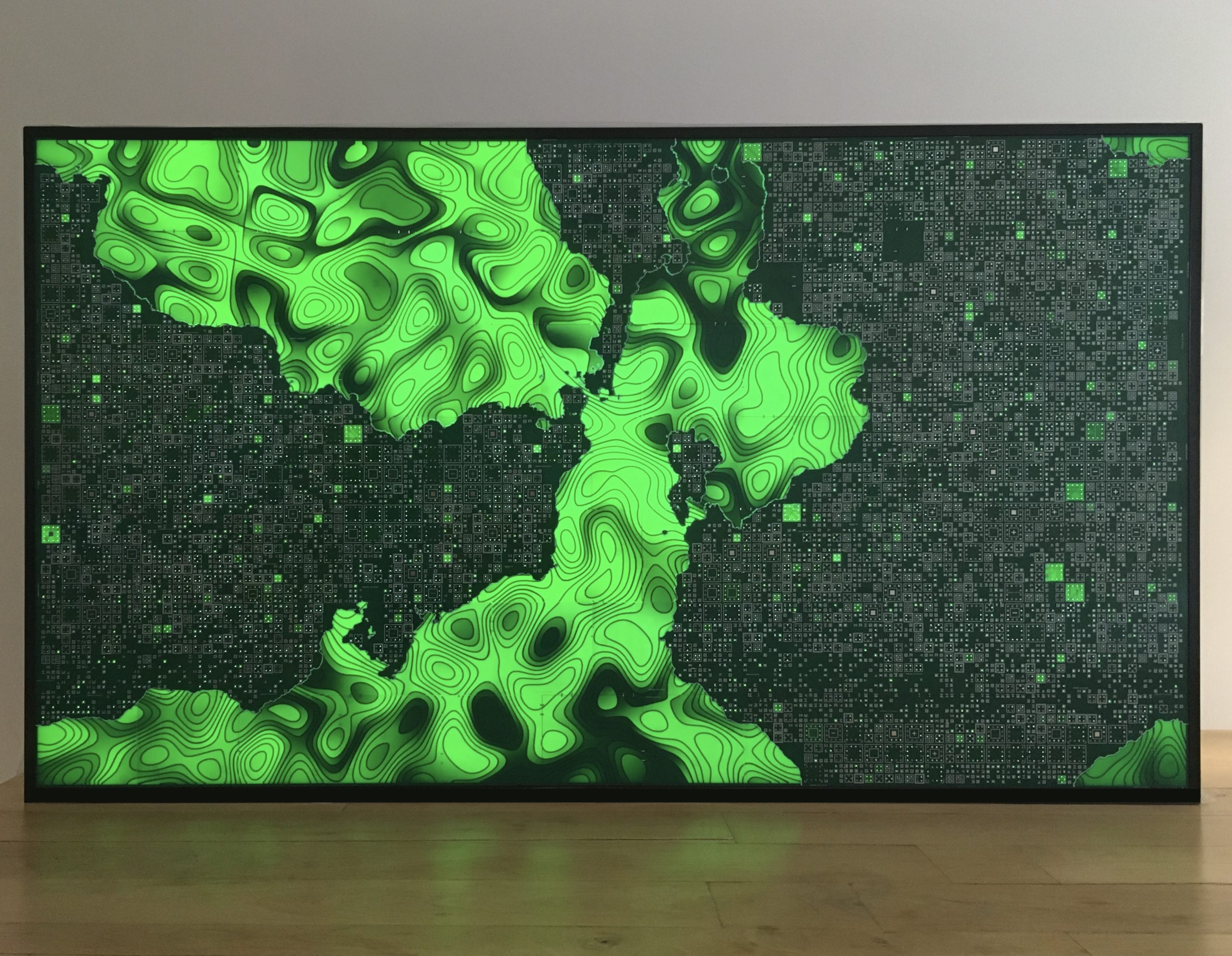
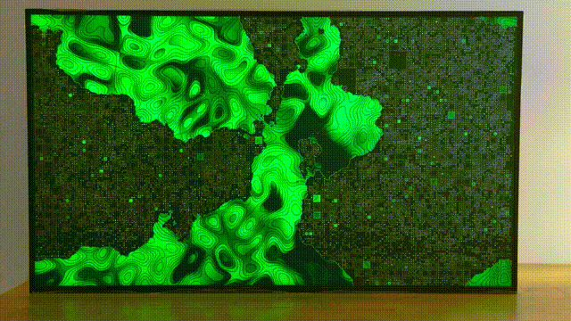
The installation will consist of a PCB layer in front of an 49″ LCD screen. By lighting pixels on the screen, specific areas of the PCB-layer will be lit / shown. Therefore the visuals on the PCB-layer and the screen will correspond strongly (and are almost identical).
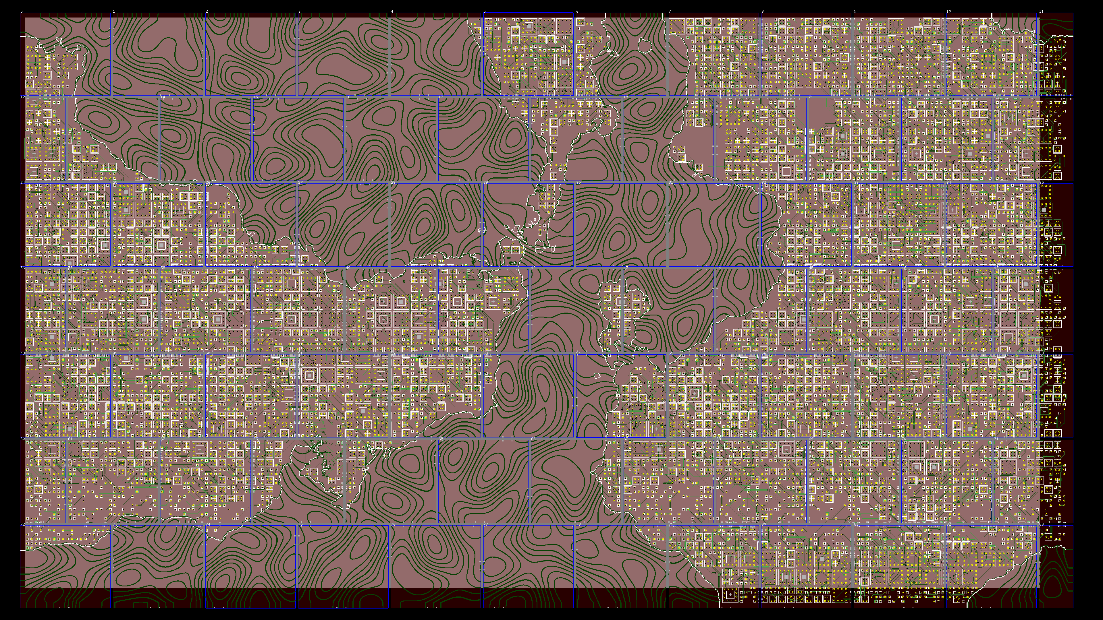
Geography
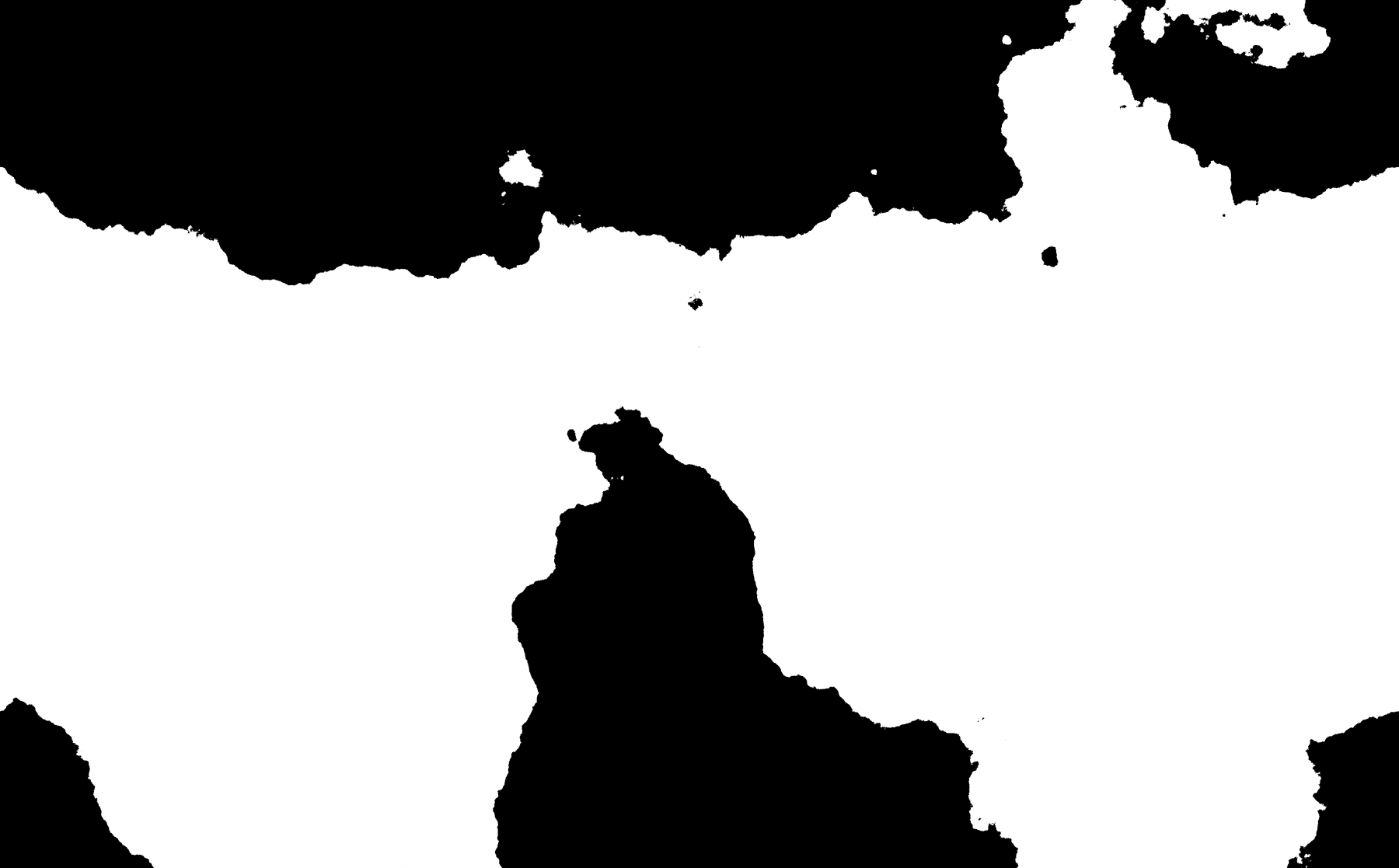
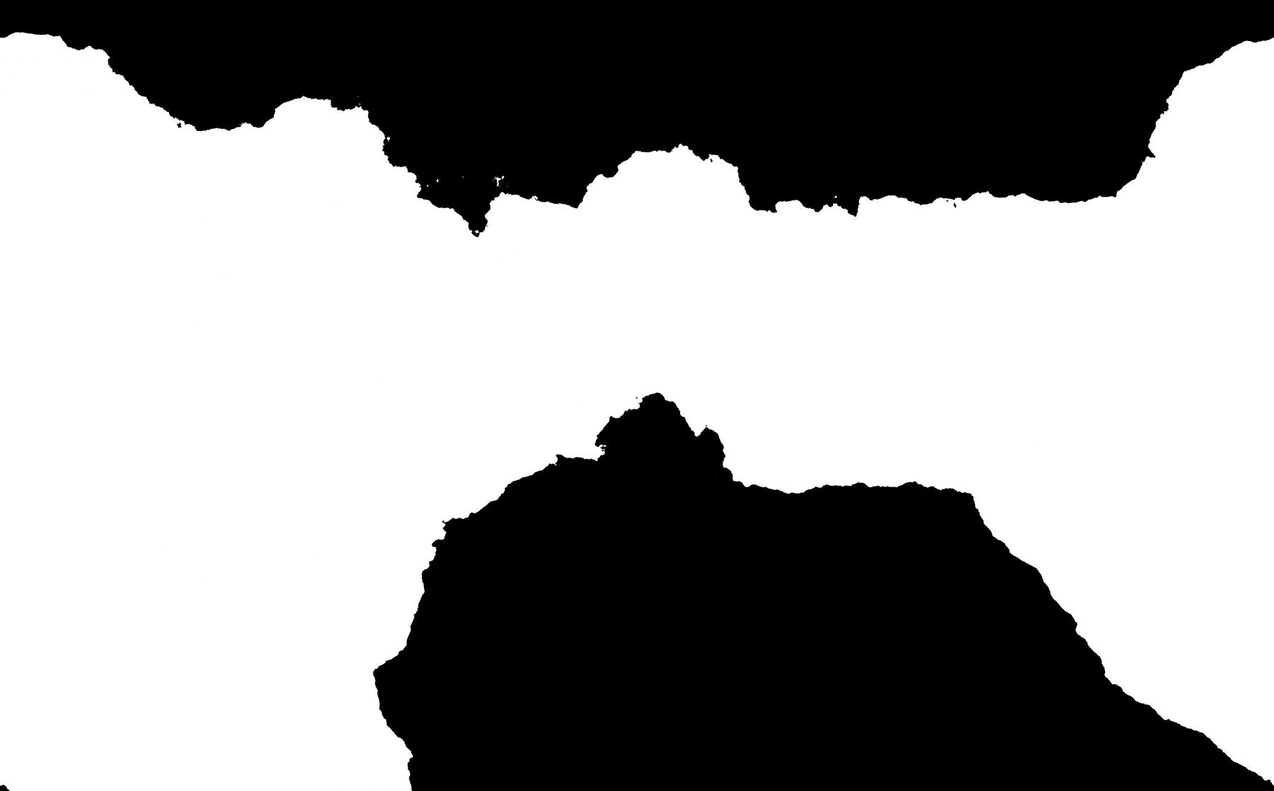
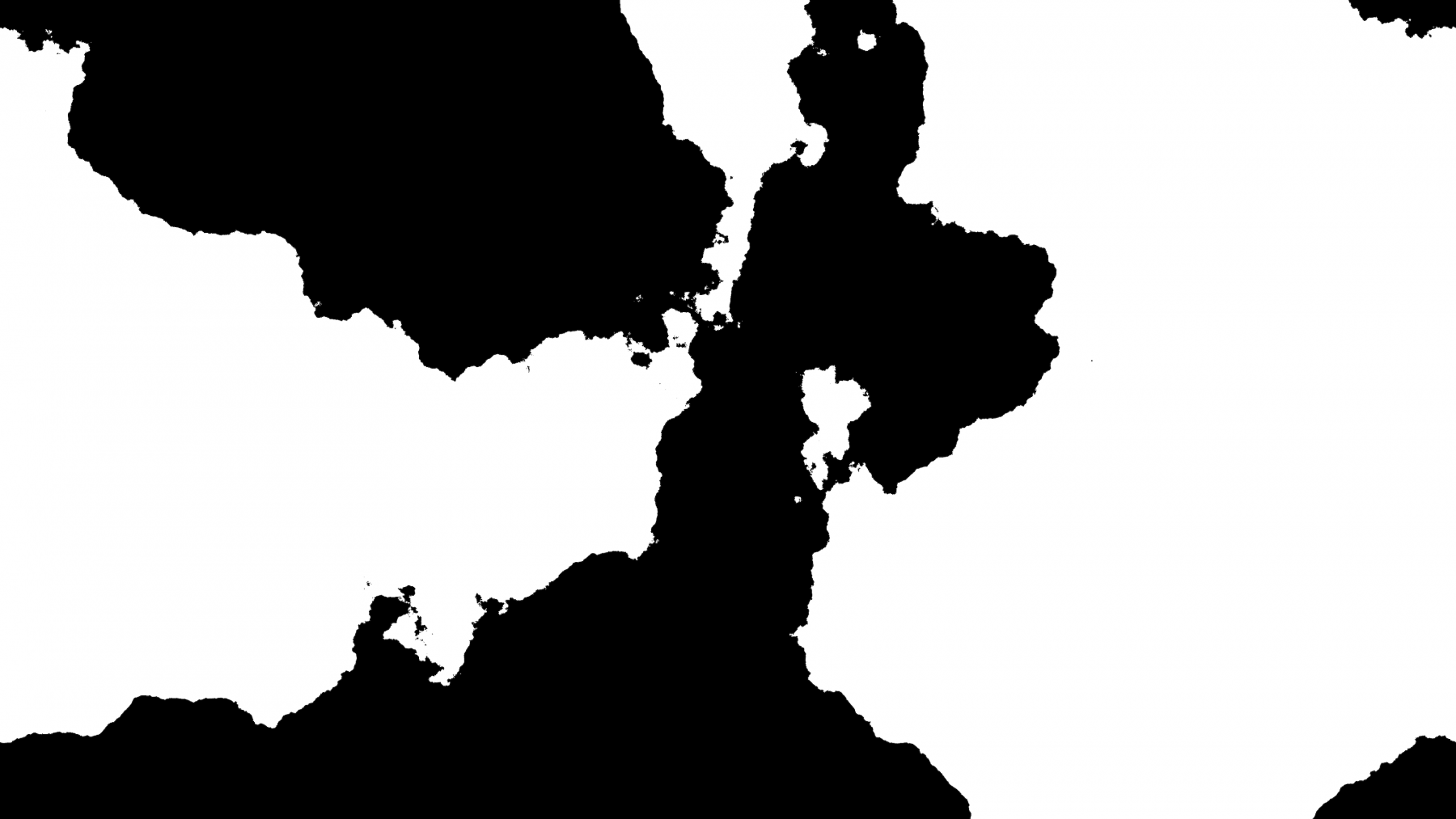
The final piece should show a reference to geography, to emphasize the relation between (global) transport and logistics. I want to generate a land/sea-like pattern. When researching this I found the wonderful Diamond Square algorithm. This starts with four points and interpolates new points between them. This recursive process is repeated a number of times.
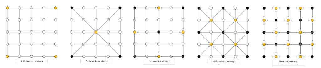
This algorithm creates a 3D structure, but I need something two-dimensional. In the 3D-model I place a black flat surface that acts like a water level. I let the program adjust the water level repeatedly until the water/land-ratio is similar to earth.
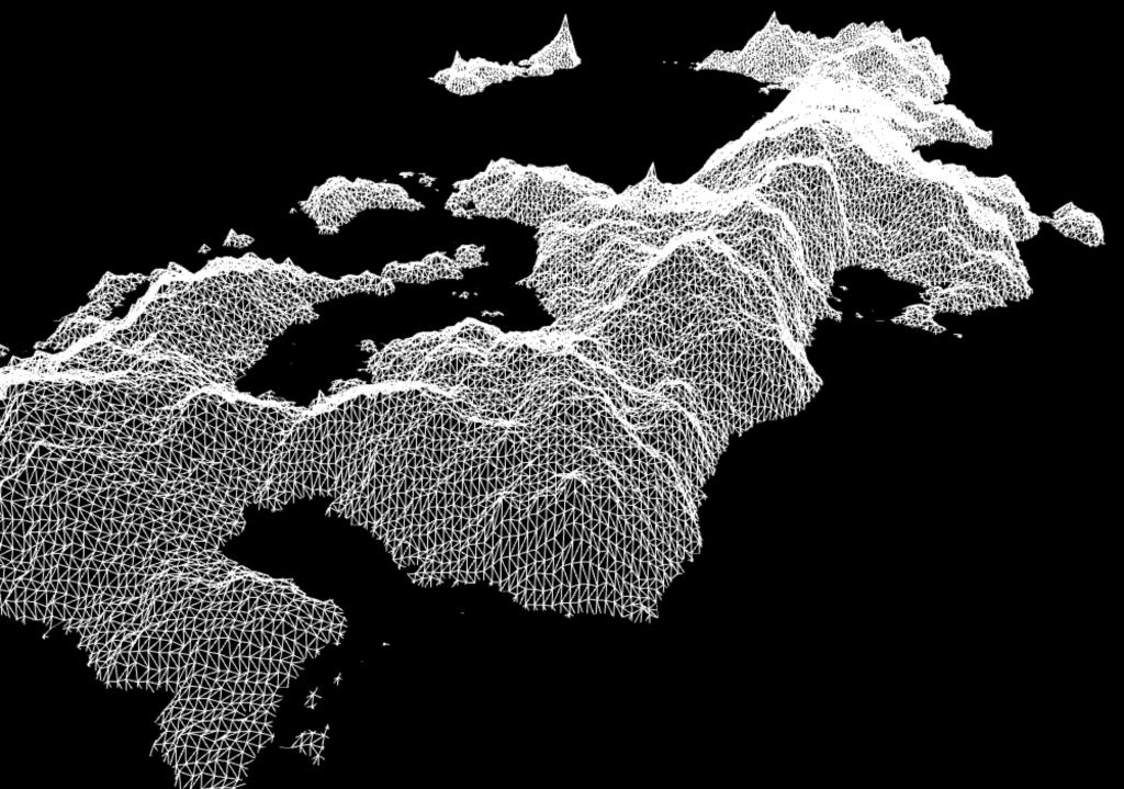
The 3D structure is rendered to a 2D drawing by checking the z-position of each point, is it above or below the water level? If it is above water, it draws a white pixel.


Using organic input
I want to have a direct reference to a natural process.
Therefore I use a photo of the Wadden-sea (The Netherlands, photo by Timo Visser).

The picture shows some unique structures and colours.
At first I try to translate the picture to simple data that refers to certain spots of constant color.
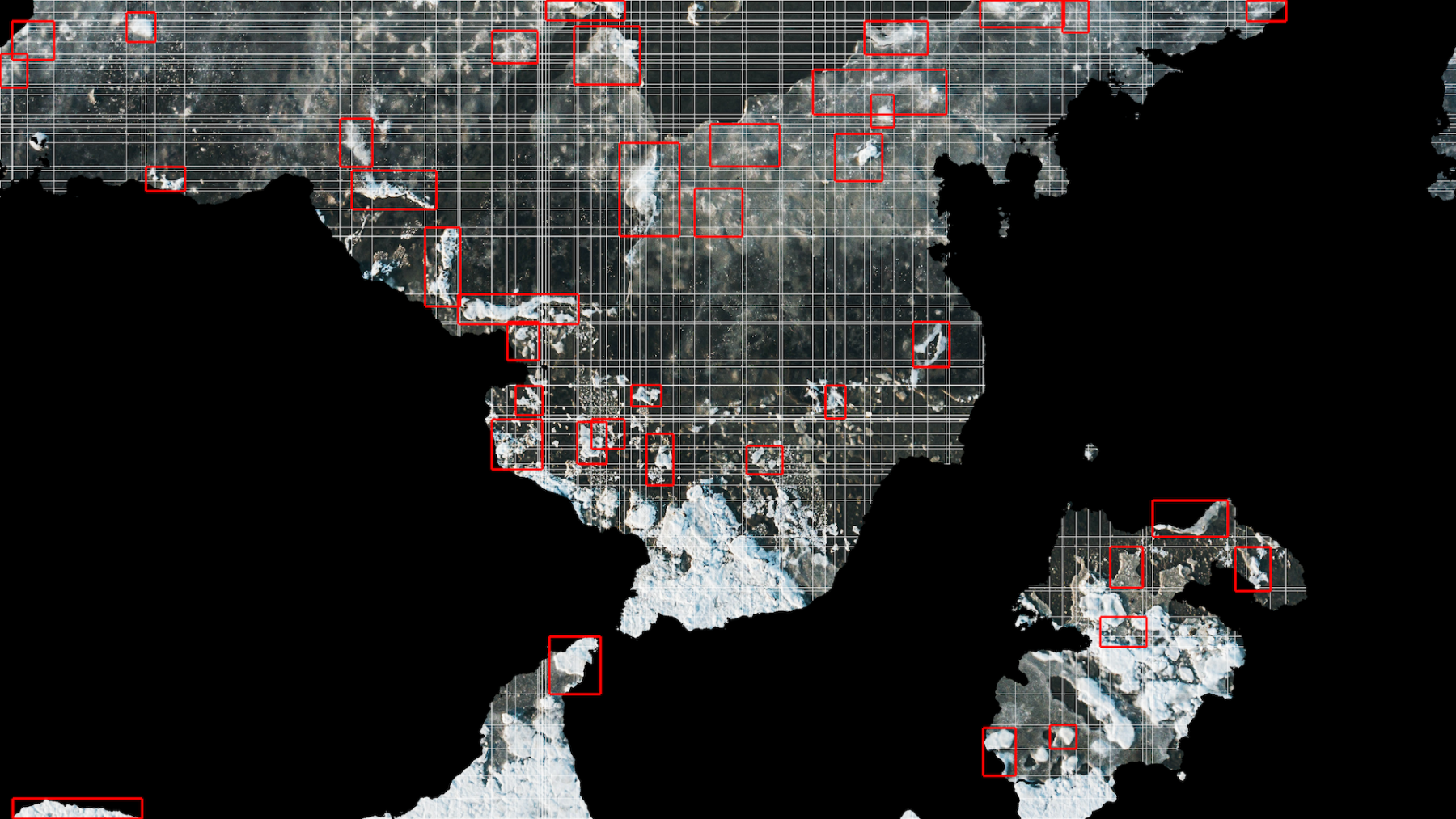
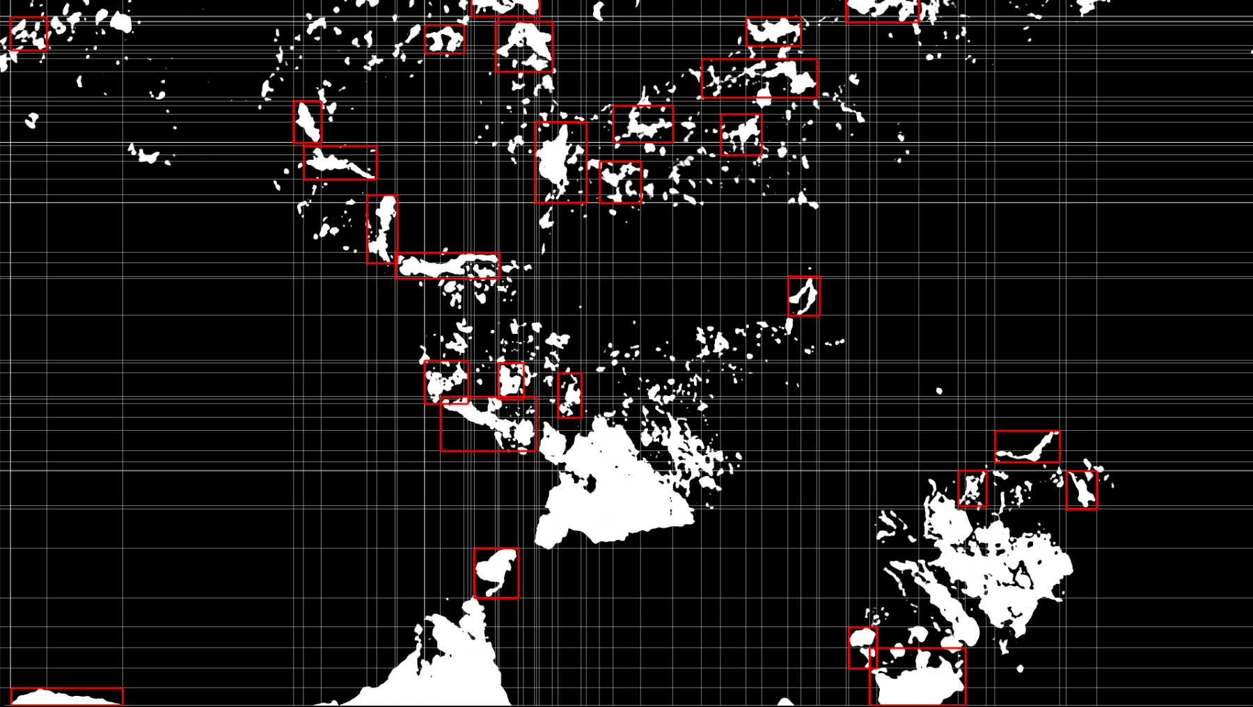
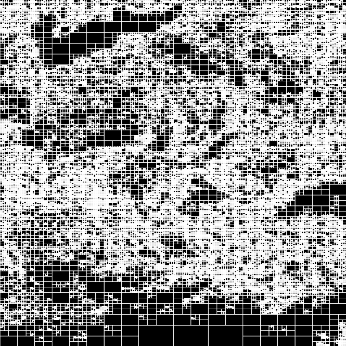
The derived data is a bit too spaced, since I want to use it for placing cities and hubs. Therefore I try another approach: translating the image to a quad-tree image.
This means that the image is analyzed on color. Sections of pixels are grouped based upon their corresponding color. This resulted in the following images.
The quad-tree image combined with the map looks like this:

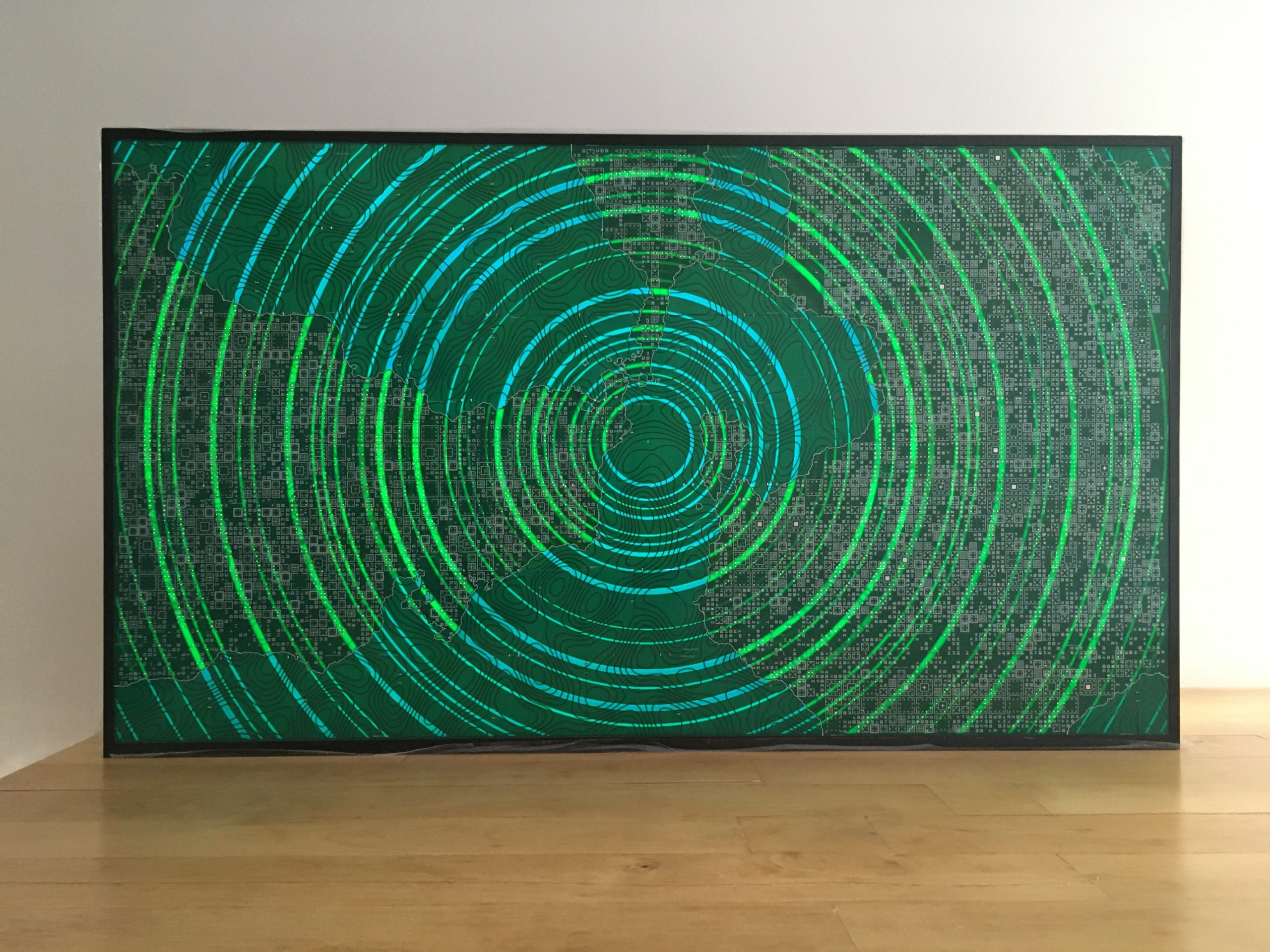
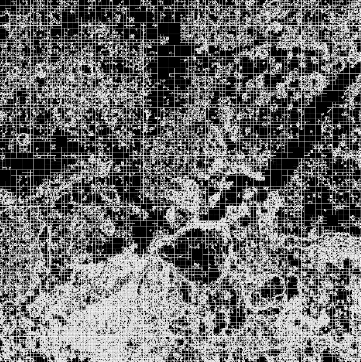
Sea appearence
For the visual appearence of the sea I’ve used a squaremarching algorithm, with Perlin Noise as an input.

The two combined:

PCB design software
To translate this design to a PCB I’ve use the open-source software KiCad. This is a fully featured program to design functional PCB’s. My goal here is to use it as an artistic medium.
I’ve chosen KiCad since it’s open-source and has a scripting capability. This means I can write my design in code.
So translating the design above is quite straightforward. A filled rectangle would be created like this (C++ to generate a Python file):
string line = "";

line += "p = pcbnew.DRAWSEGMENT()\n";

line += "p.SetLayer(layertable['"+layerNames[layerID]+"'])\n";

line += "p.SetShape(pcbnew.S_POLYGON)\n";

line += "points = pcbnew.wxPoint_Vector()\n";

for(char i=0; i<5; i++){

    line += "points.push_back(pcbnew.wxPoint(pcbnew.FromMM("+ofToString(pixelToMm(coords[i][0]))+"), pcbnew.FromMM("+ofToString(pixelToMm(coords[i][1]))+")))\n";

}

line += "p.SetPolyPoints(points)\n";

line += "p.SetWidth(int(pcbnew.FromMM(0.00127)))\n";

line += "board.Add(p)\n";
The full KiCad python API can be found here.
Connections / traces
The blocks on the map reflects hubs, cities or likewise entities. My final goal is to visualize traffic between these places. Therefore I have to create some connections. Almost all entities are connected via each other.


To give these lines an actual PCB-like visual appearance I’ve used freeroute. That’s software that generates traces on actual PCB designs. It connects all the straight lines in the image above with typical 45-degree-angled lines.

Each rectangle has its own look: number of holes, lines and accents. The width of the traces is matched by the size of one pixel.

Manufacturing
Tiling
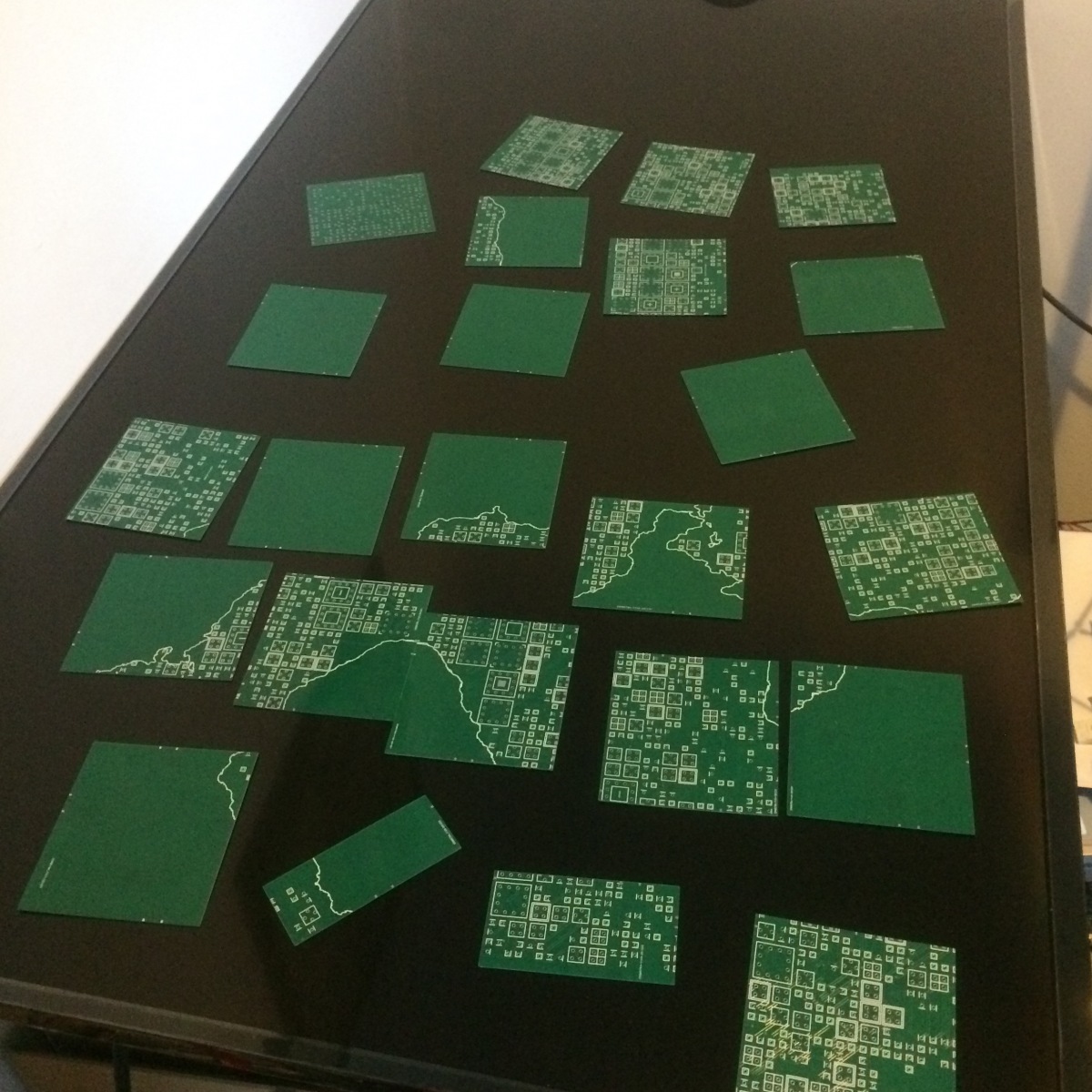
The PCB layer won’t be one solid 66x112cm piece. It isn’t possible to get a 0.6mm PCB of this size manufactured. So it will consist of multiple parts (<10x10cm). It’s also more genuine to keep the PCBs small, as they usually are of small dimensions.

The challenge is to divide the full scale design into different small PCB’s.
All lines on the PCB are checked if they’re within a certain range, like this:

This way the whole design has been divided in certain sub-sections.
A single board looks like this (Board #70, top view):

Assembly
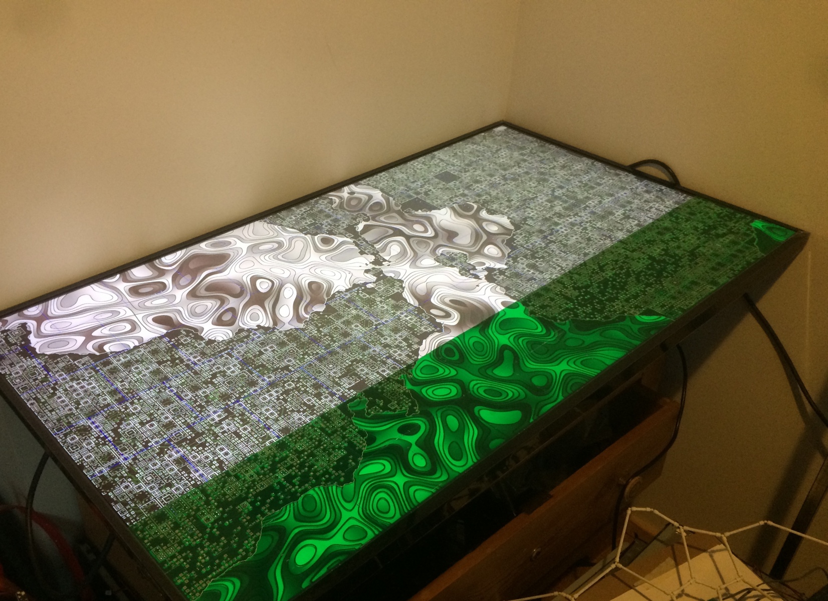
All the seperate PCBs are arranged and then soldered together into one big PCB.